One of the biggest challenges SMT assemblers are facing is the need to control the quality of a printing process. More than 70% of the assembly failures are rooted in this critical production- phase. When dealing with complex PCBs containing a large number of micro BGA and ultra-small chip components, or those based on a wide use of step stencils, flexible panels, etc – the challenge intensifies. If you wish to avoid potential failure opportunities, such as shorts between adjacent pads, or variance of solder paste volume, you must first optimize the process parameters, but it needs to be followed by a well reliable process control method. You need to get the right amounts of solder paste, but also make sure it is repeatable and statistically stable.
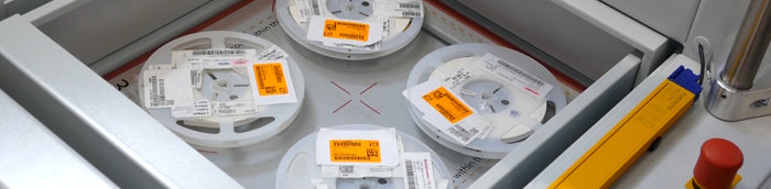
The best method of solder paste inspection is to be able to use the SPI results for a rebalance of the process. That way you can improve all the time. Solder paste is a mixture of powdered metal particles spheres held within a flux paste base. There are numerous solder paste materials you can choose from. Using the correct type of solder paste is usually based on your customer needs and industry definitions, but the optimization and the reduction of failure opportunities come from experience and knowledge. AMS Electronics is well-known for its pioneering approach when it comes to trying new methods, and materials aiming for the best results in the shortest possible time.
SMT soldering process is comprised of a few standard steps:
1. Laying a bare PCB in the machine (set-up, support methods, etc.).
2. Implementing the pre-designed DFM solder stencil apertures to the board, thus controlling the way the solder paste is applied, and preventing failure opportunities.
3. Controlling the printing machine parameters such as squeegee pressure, standoff height, squeegee speed, stencil release, cleaning cycle parameters, and more.
4. Assembling the components on top of the solder paste printed board using the pick & place machine.
5. Reflowing the solder paste with a well-controlled solder profile.
Experience has shown that you need to master not only the knowledge of the solder paste types but also the robustness of the DFM (Design for Manufacturing) of your PCB. The larger its scale – the more issues it can tackle later on in the assembly process. For instance – soldering a thermal pad for "gullwing lead shape, SOP" component can be addressed in the early stages of the DFM while designing a stepped or an over-print stencil for its application. At the same time, increased stencil height might increase the solder paste application failure rate for a nearby 0.35 pitch BGA. It’s a very elusive balance.
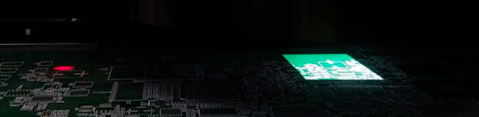
Today’s miniaturized popular components (01005 - 0.4mmX0.2mm, 0201 –0.6mmX0.3mm, 0.32mm or 0.35mm pitch WLCSPs, etc.) pose an even greater challenge to the soldering process. You need to apply the paste in tiny holes through the stencil with a very low area ratio (less than 0.66), which can no longer be seen by the human eye, sometimes not even through a microscope. In other cases, when traditional large-sized components are used with the same PCBA, you need to allow stability for extra volume to make sure a good and reliable solder joint is created. In the past, the process has been visually inspected with a 2D inspection machine or additional software application for the printing machine. Unfortunately, these options, only cover the top projection of the board. Today, a 3D cutting-edge SPI machine (manufactured by A-Leader) supplies the missing in-depth visualization of the printing process. Surrounding light projection enables the detection of all side view surfaces thus literally shedding light on the height and volume of the solder aperture.
Using the SPI machine provides our customers with invaluable advantages:
1. Bottom Terminal Components (BTC) use becomes more frequent. Once the components are placed on top of the solder paste their failure, if occurring, can no longer be traced. The only way to detect failures is using X-ray post reflow, but this might be proven as too late in the process. When the BTC is already reflowed, it is very difficult to find a printing root cause, and it can lead to non-stable production quality. 3D SPI detects volume and height printing failures, which prevents failure opportunities, and most importantly, helps avoid future failures, thus constantly improving your scores.
2. The machine is capable of documenting the soldering process in its entirety, enabling root cause analysis.
3. The above materialize into money savings, decreased number of time-consuming processes, and increased yields, production quality, and OTD capacity.
4. Errors-tendency is relatively easy to detect. The machine can trace a repeated error, thus allowing an optimized correction process. This becomes crucial when dealing with prototypes. Using brand new, complex components on the one hand, and aiming for development completion in the shortest possible time, on the other - requires stability and repeatability.
5. High Mix Low Volume (HMLV) compatibility – 3D inspection makes repeated portions trials redundant. The machine supports a very flexible production process with high ”quick turn-around”, and is up and running in no time when assembly lines should be altered. It only takes minutes to reprogram a full inspection coverage or adjustment tolerances. At the same time, the level of precise and accurate measurement is maintained, not to mention easy and transparent reporting and defect verification.

A clear distinguish between the pastes, pads, silkscreen and the board

Accurate and noise-resistant measurement of the paste height and volume